P·04 · Electrical
STM32 6S FOC Motor Controller
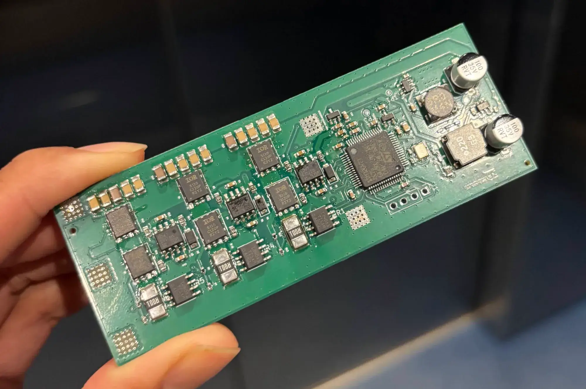
A four-layer sensorless field-oriented-control (FOC) ESC for a 340 KV drone motor, laid out to keep current sensing clean beside the switching stage.
At a glance
- ~1 monthfrom blank schematic to a finished four-layer layout, solo
- 4 railsgenerated on-board from the 6S pack: 12 V, 5 V, 3.3 V digital, 3.3 V analog
- 99%design efficiency at 80 W
- Where
- Geolabs, Inc.
- Role
- Sole designer (schematic and layout)
- Team
- Solo
- Timeline
- About 1 month of design
- Status
- Complete
- KiCad
- 4-layer PCB design
- STM32 (STM32G473)
- Field-oriented control (FOC)
- Sensorless BLDC control
- Gate drivers
- Shunt current sensing (INA240)
- Buck converters and LDOs
- Signal integrity
- PCB thermal design
- SMD hot-air rework
The problem
I designed this electronic speed controller (ESC) for Geolabs’ drone work. The goal was a compact, thermally stable, low-noise controller for drone propulsion, where weight and throttle response matter. The brief I worked to:
- Input: 6S Li-Po, 25.2 V fully charged.
- Motor: a 340 KV brushless DC drone motor.
- Control: field-oriented control (FOC) for smooth commutation and fast torque response.
- Rails: 12 V, 5 V and 3.3 V all generated on the board from the pack.
- Board: compact enough for a drone frame, on a low-cost four-layer process, on a limited budget.
- Time: one month for circuit design, part selection and layout.
The hard part is that the board has to measure phase current accurately while it switches large currents a few millimetres away. FOC is only as good as its current measurement, so most of the design effort went into keeping the sense path clean.
Approach
Sensorless FOC on an STM32G4
The control loop is designed to estimate rotor position from phase current and back-EMF, so the motor needs no position sensor. That puts the load on the microcontroller. I picked the STM32G473 for its hardware floating point, fast ADCs, and the advanced timers that generate complementary PWM for three half-bridges.
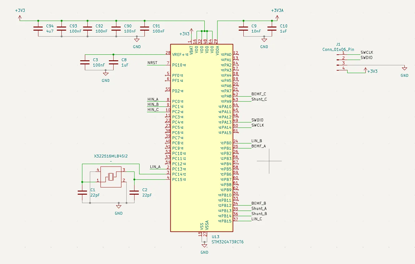
A stepped power tree with a separate analog rail
Every rail comes off the pack in stages, each one sized for what it feeds:
| Rail | Made by | Feeds |
|---|---|---|
| 25.2 V | 6S pack directly | the three half-bridges |
| 12 V | buck converter from the pack | gate driver |
| 5 V | second converter from 12 V | current-sense amplifiers and sensors |
| 3.3 V | low-noise LDO from 5 V | STM32 |
| 3.3 V analog | its own LDO | sensor and ADC references |
I chose 12 V for the gate rail because that is where most half-bridge gate drivers give full enhancement on N-channel MOSFETs. The analog reference gets its own LDO instead of sharing the digital 3.3 V, so logic switching noise can’t couple into the current measurement.
Shunt sensing on every phase
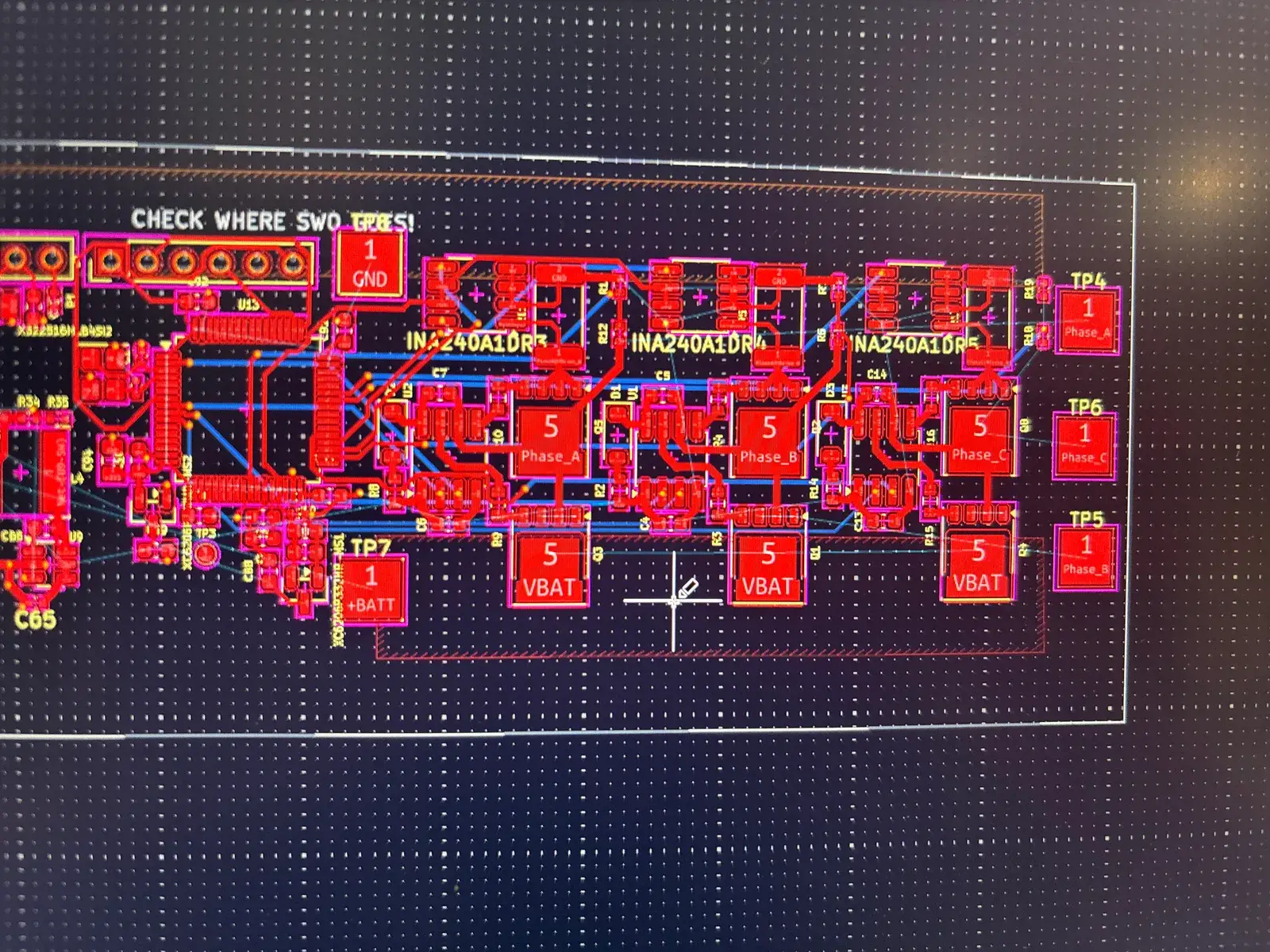
Each phase has a low-resistance shunt read by an INA240A1 current-sense amplifier straight into an STM32 ADC. Three independent measurements are what let the FOC loop balance phase currents. The gate driver has built-in dead time and bootstrap supplies, and I tuned the pre-driver for minimal switching delay so the three phases stay in step.
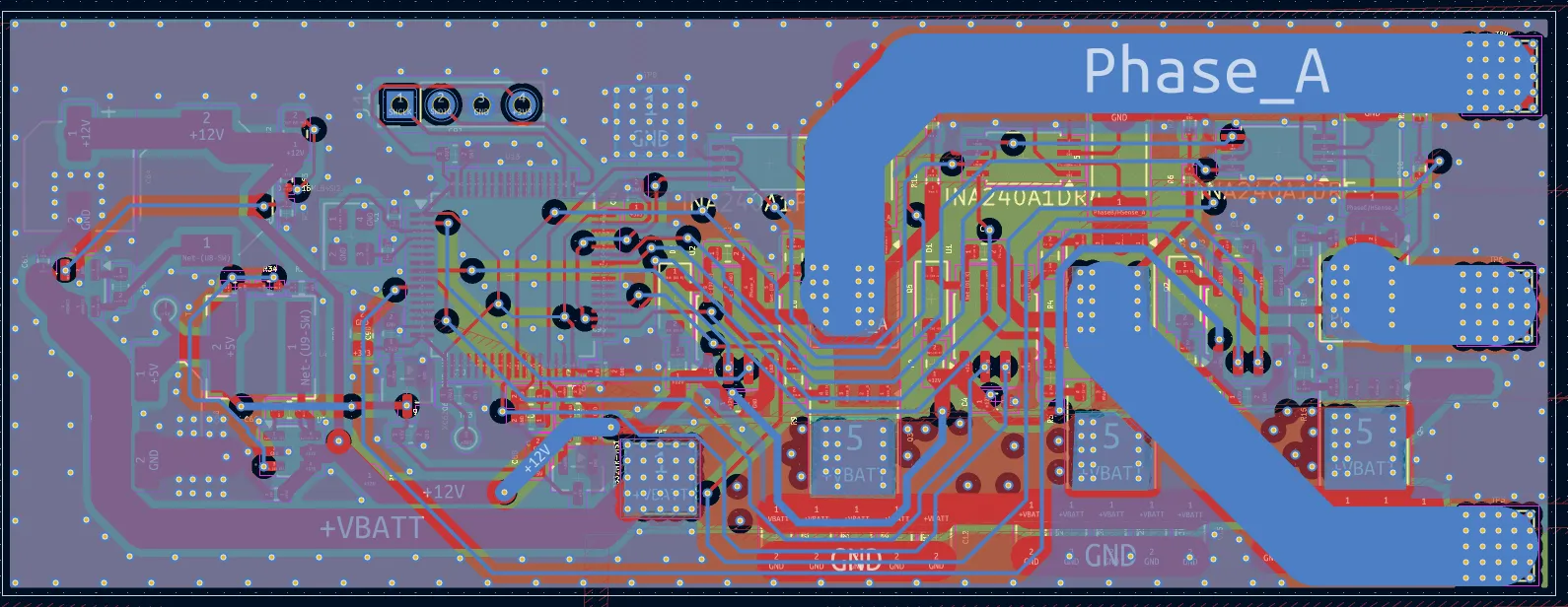
Four layers, solid ground
| Layer | Use |
|---|---|
| L1, top | signal and power |
| L2 | continuous ground plane |
| L3 | gate-drive routing |
| L4, bottom | signal |
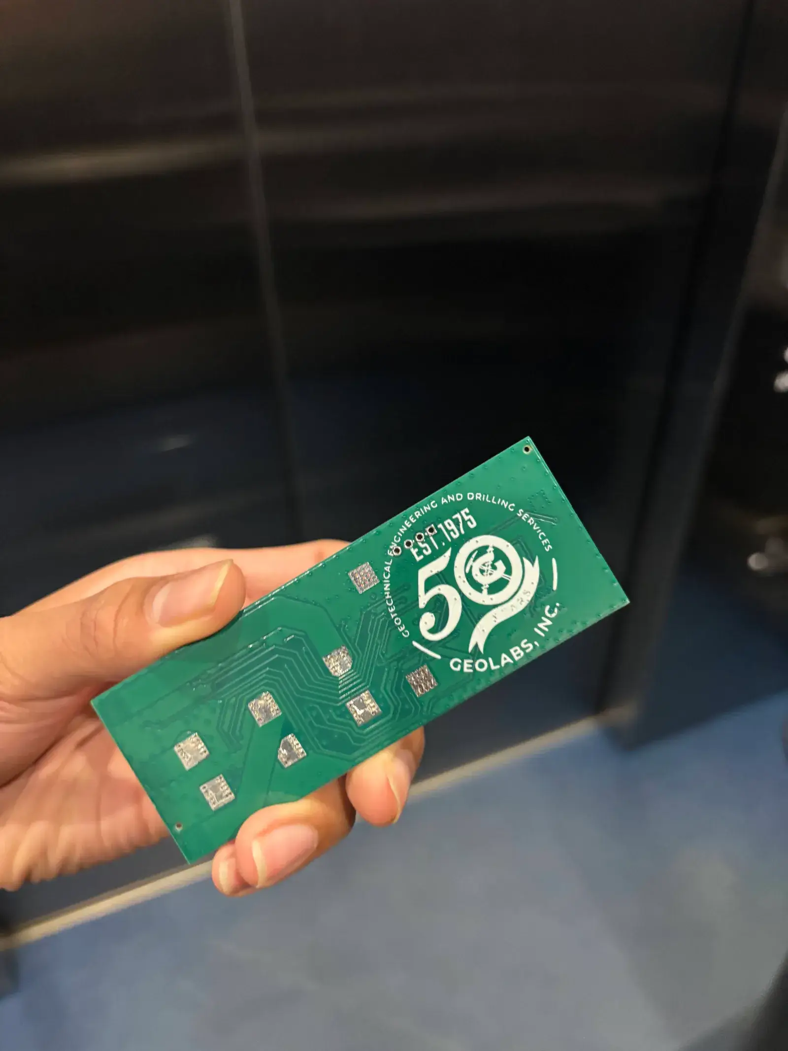
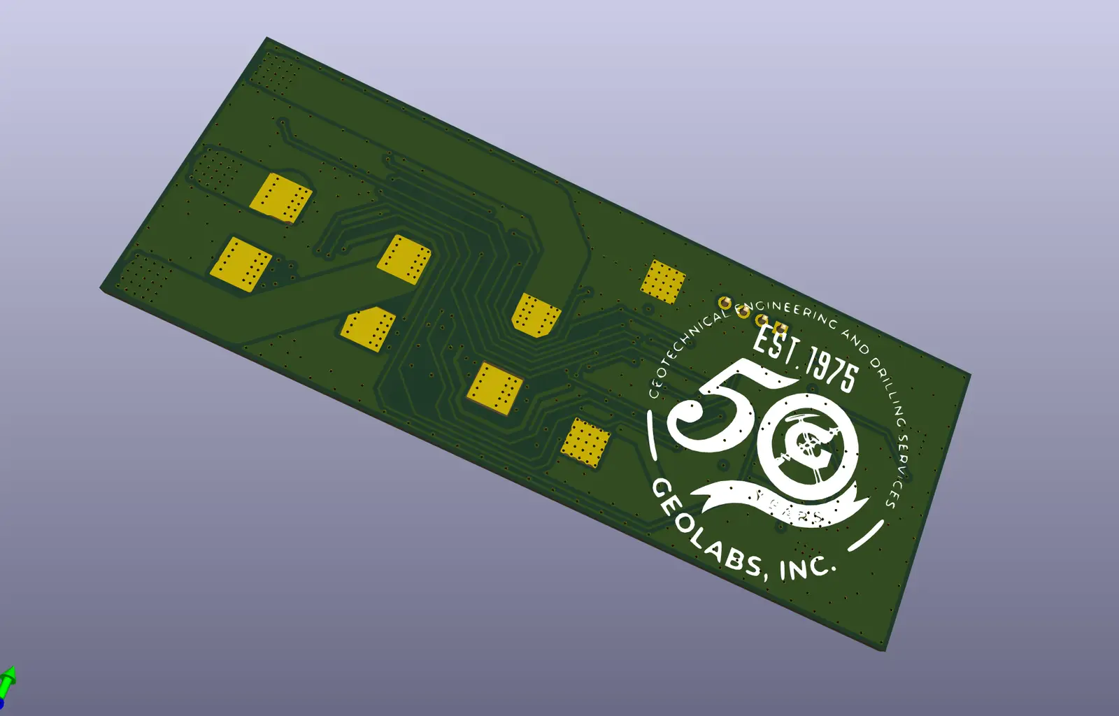
Four layers was the compromise between EMI shielding and fabrication cost. I kept the ground planes solid and rejected partial copper cuts, because a cut plane makes return currents detour and forms the inductive loops I was trying to avoid.
Engineering detail
The high-current loop
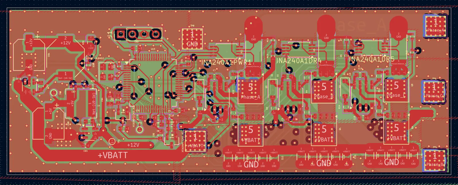
The path from the pack through each half-bridge and back to ground is the loop that sets switching loss and ringing, so I kept it as short and wide as the footprint allowed. Stitching vias line the edges of the high-current regions to hold down ground bounce.
Heat
The MOSFETs sink heat into copper pours on their drain and source pads, with thermal via arrays underneath that carry it into the internal planes. I sized trace widths and via counts to the current each net carries, and shortened and widened the main power traces to keep their impedance low. The MCU also monitors bus voltage and its own temperature and is designed to scale PWM duty down when either drifts out of range, so the controller backs off before it overheats.
Noise
- The current-sense feedback runs as differential pairs where possible, routed away from high-di/dt power traces.
- The STM32 crystal has short, symmetric traces and sits away from the switching nodes to limit jitter.
- Local bypass capacitors sit within 2 to 3 mm of each IC power pin, with high-frequency ceramics in parallel with bulk capacitors.
- The noisy digital section is fenced off from the analog front end with ground copper.
- I tested buck-inductor positions and orientations to keep its field and eddy currents away from sensitive traces.
Fitting the drone
Connectors, mounting holes and the three phase outputs are placed to match common drone-frame geometry. Spacing and clearances follow the fab house’s limits while holding safe creepage for the 25.2 V domain.
Build
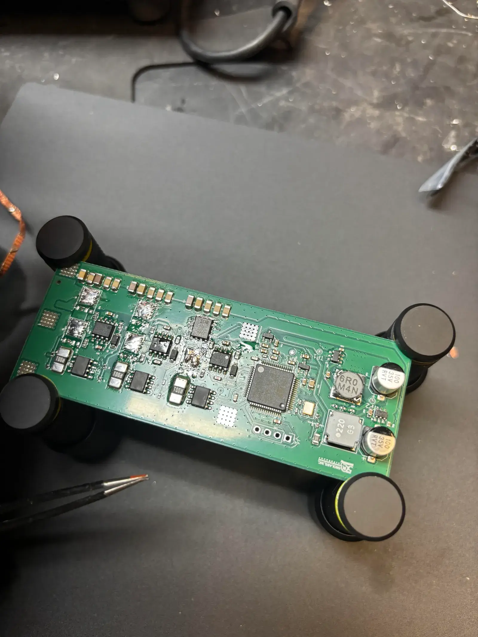
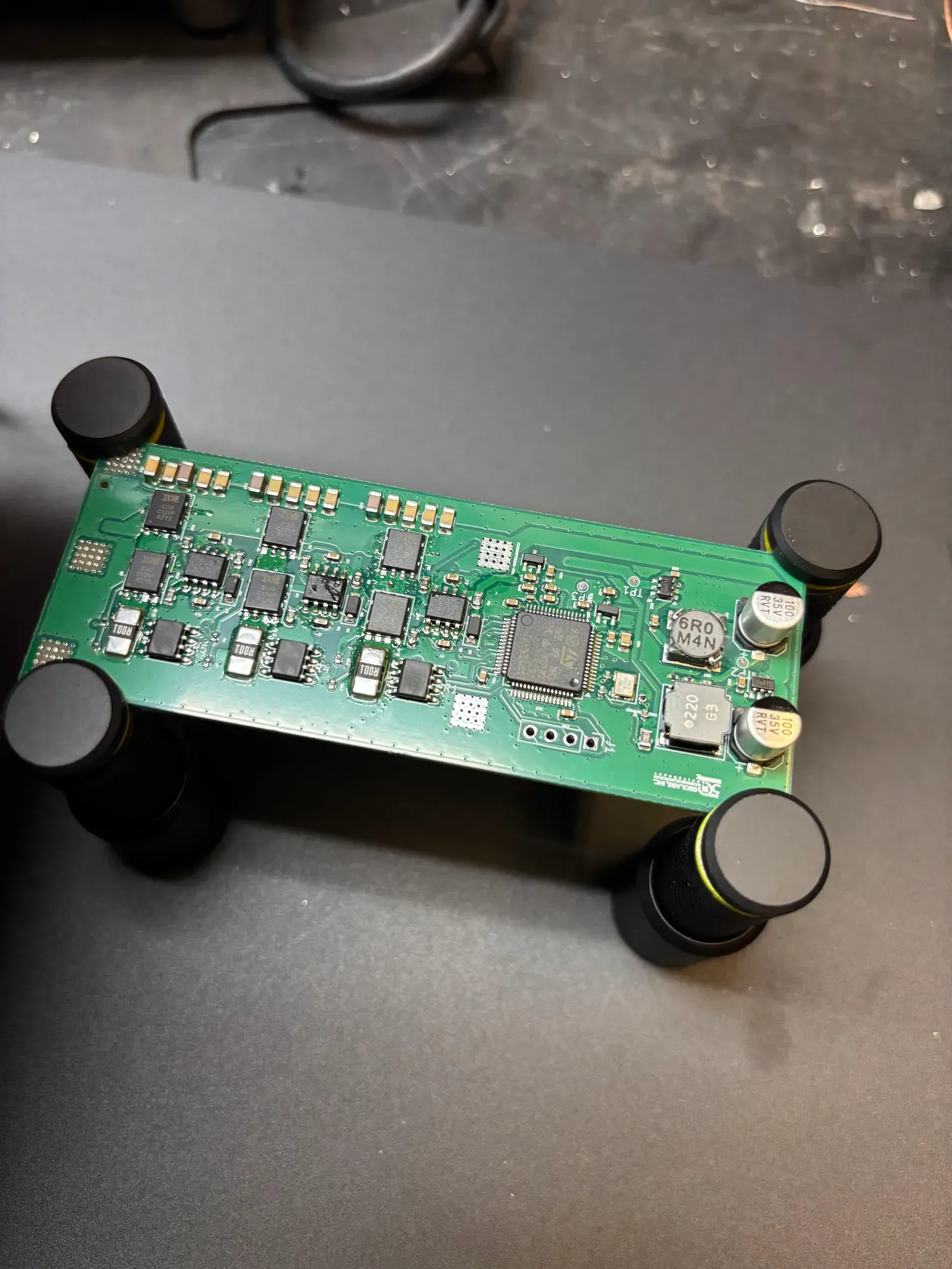
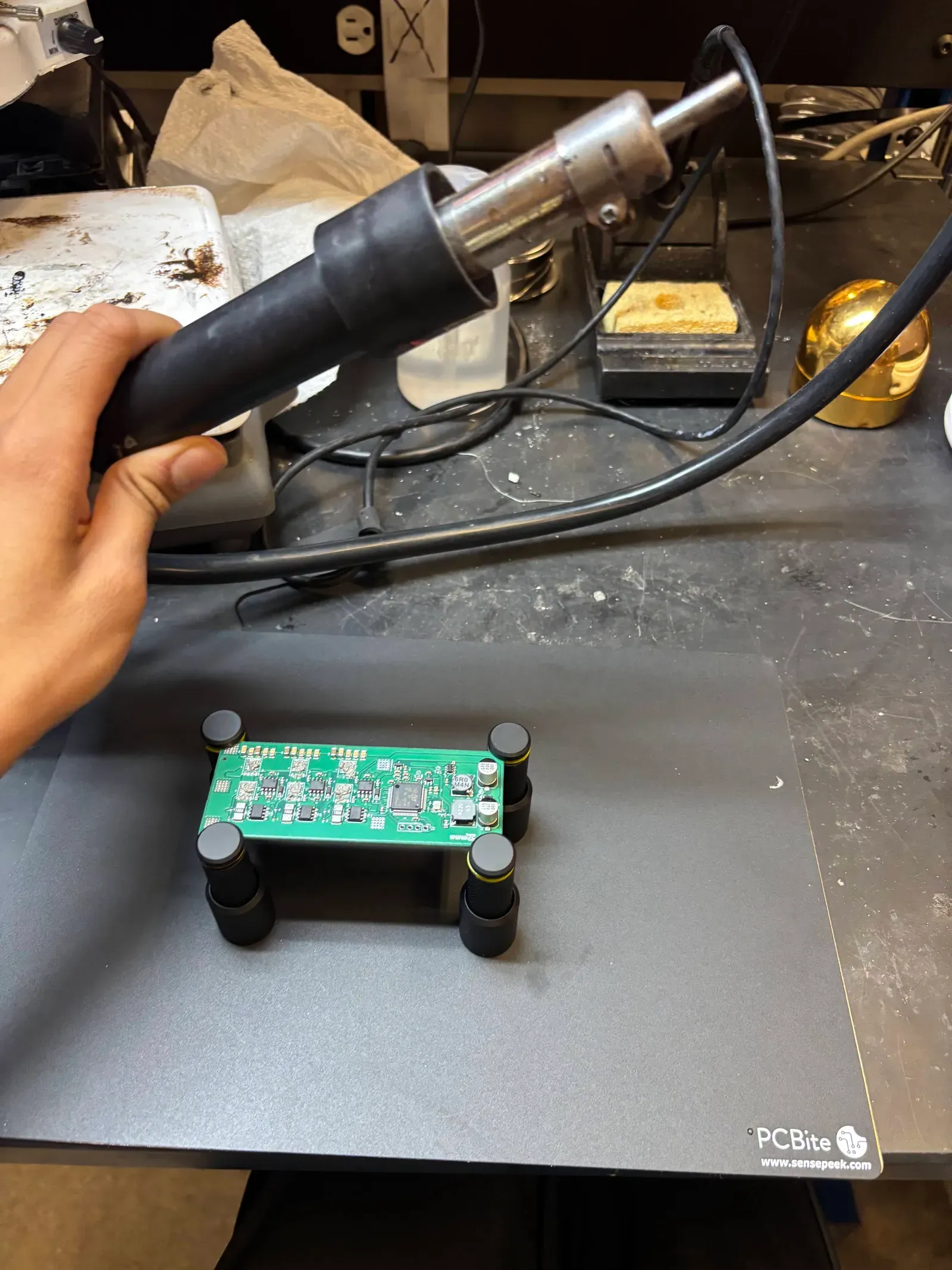
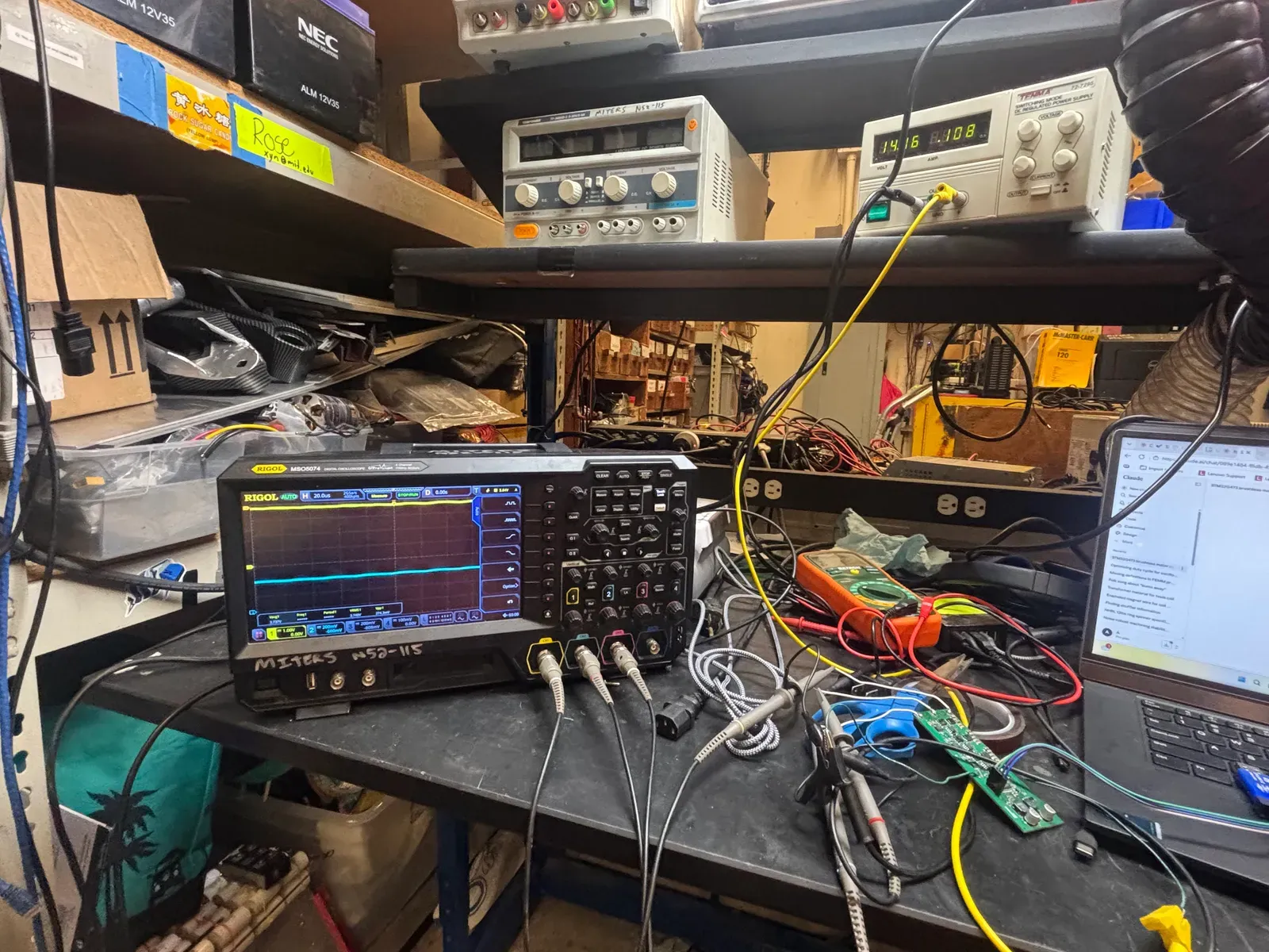
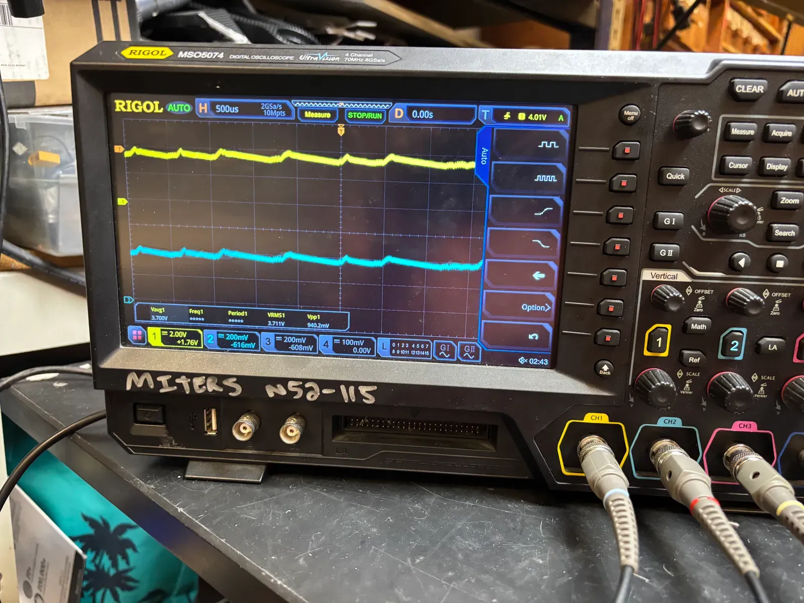
After fabrication I assembled the board, reworked parts with hot air where needed, and set it up on the bench with a bench supply and an oscilloscope.
Results
- Designed for 99% efficiency at 80 W on a 6S pack.
- Schematic, part selection and a four-layer layout finished in about a month, alone.
- Fabricated and assembled, with every rail generated on the board.
My contribution
I did this project alone, for Geolabs: requirements, schematic, part selection, the four-layer layout in KiCad, and assembly.
Gallery
4 images